

Everything You Need to Know About Electronic Boards
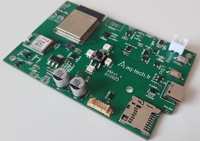
At AQ-Tech, most of the products we design include an electronic board. Whether it is time display, temperature sensing, signal acquisition, LED driving or Internet connectivity, electronics sit at the core of the system. Our engineering team designs, prototypes, tests and validates dozens of boards every year for connected sensors, IoT devices, user interfaces and embedded systems. This guide gives you a clear understanding of what a PCB and a PCBA are, the main PCB types and components, and the best practices from design to industrialization.
Contents
- 1. PCB/PCBA: key definitions
- 2. A short history
- 3. Major PCB types
- 4. Component families
- 5. From idea to product: design, prototyping, industrialization
- 6. What to watch: reliability, sourcing, costs
- 7. Conclusion
1. PCB/PCBA: key definitions
A typical “electronic board” combines a PCB (Printed Circuit Board) with components soldered onto it; the assembled set is a PCBA (Printed Circuit Board Assembly). The PCB provides both mechanical support and electrical interconnects using copper layers. Modern boards often include several layers to route power and signals while preserving signal integrity and EMC performance.
The board stacks conductive copper and insulating dielectric layers, with vias connecting them. Components can be placed on the top and/or bottom side. A sound design ensures excellent electrical performance at controlled cost and lead-time, with repeatable quality in production.
2. A short history
From early hand-wired assemblies to today’s multilayer HDI boards, PCB manufacturing has dramatically evolved. Switching from wire harnesses to etched copper traces enabled industrial scale and repeatability. Today, high-density boards pack many layers into a few millimeters, making advanced embedded electronics possible in compact products.
3. Major PCB types
Layer count: higher counts allow cleaner routing (power distribution, ground planes, differential pairs) but increase cost. Two layers are fine for simple devices; 4–8 layers are common for complex embedded, RF and high-speed systems.
Single/double-sided assembly: placing components on both sides reduces footprint but adds assembly complexity.
Thickness & materials: 1.6 mm is common, with thinner 1.0 mm or specific stackups when mechanical constraints apply. For thermal management (LEDs, power), aluminum-core PCBs are used. Flexible boards (FPC) enable textile integration and complex shapes; rigid-flex combines both worlds.
4. Component families
Through-hole (THT): leads inserted into plated holes and soldered. Robust for connectors, electrolytics or power parts, but less suited to very high-volume automated assembly.
Surface-mount (SMD/SMT): the industry standard for miniaturization and automated assembly (0402/0603 passives, QFN, BGA…). Complex packages (fine pitch, bottom pads) demand tighter manufacturing control (stencil design, reflow profile, AOI, X-ray for BGAs).
5. From idea to product: design, prototyping, industrialization
A robust path typically includes:
- Requirement capture: functions, interfaces, mechanical envelope, environment, target standards.
- Electronics architecture: MCU/SoC choices, analog/digital split, power tree, sensors, RF, storage, connectivity.
- Schematic & layout: DRC rules, controlled impedance, ground planes, decoupling, sensitive zones (analog/RF).
- DFM/DFT: design for manufacturing & test (test pads, debug ports, in-system programming).
- Prototyping & verification: functional checks, characterization, pre-compliance EMC, robustness.
- Industrialization: frozen BOM, fab packages, test jigs, traceability, ramp-up to series.
We help teams speed up this cycle with our Electronics & Firmware, Prototyping & Testing and Industrialization & Certification services, ensuring a smooth handover to Manufacturing when the product is ready.
Special cases: technical textiles & compact embedded
For wearable or material-integrated devices, boards must be thin, light and robust. Our Smart Textile hub combines flex/rigid-flex PCB design, reliable interconnects, low-power management and wash/wear constraints. This expertise also benefits medical & well-being and sports & lifestyle applications.
6. What to watch: reliability, sourcing, costs
Reliability & EMC: proper ground planes, return paths, decoupling and analog/RF isolation reduce noise and emissions. Early pre-compliance tests save expensive iterations later on.
Critical parts: availability (lead-times, obsolescence) directly impacts schedules. Standardizing key references, qualifying alternatives and maintaining a safety stock mitigate shortages. A BOM with cross-references and parametric windows reduces redesign risks.
Total cost: driven by PCB area, layer count, drills/vias, tolerances, assembly plan (single/double-sided), machine time and scrap rate. A design-to-cost approach with the factory keeps budgets under control.
7. Conclusion
Understanding PCB/PCBA structures, board types and components, plus DFM/DFT logic, is essential to turn ideas into reliable products. Have an electronics project? Let’s talk with our Electronics & Firmware team. We can frame your needs, prototype fast and support your industrialization journey.
Want to dive deeper? Explore our Prototyping & Testing and Manufacturing pages, or contact us.
