

Understanding How Electronic Boards Are Manufactured
Electronic boards are at the core of most modern products — from connected objects and industrial sensors to medical devices and consumer electronics. Understanding how they are manufactured helps anticipate technical constraints, improve reliability, and control production costs. After exploring the basics of PCB design in our previous article, let’s now look at how a printed circuit board is actually produced.
Contents
- 1. From design to manufacturing documentation
- 2. PCB production steps
- 3. Component soldering and assembly
- 4. Quality control and functional testing
- 5. Best practices for reliability and cost control
- 6. Conclusion
1. From design to manufacturing documentation
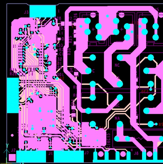
Everything begins with the design office. Using electronic CAD software such as Altium Designer, KiCad, Proteus, or Eagle, the engineer defines the product’s electrical schematic, interconnections between components, board shape, layer count, and dimensions. The goal is a design that’s both technically sound and ready for mass production.
Once the design is validated, the next step is to generate a complete manufacturing package (also called an industrialization file). This documentation is sent to a manufacturing partner — known as an EMS (Electronics Manufacturing Services) — responsible for producing and assembling the board. It includes:
- Gerber files: describing all PCB layers (copper, solder mask, silkscreen, outlines, and drill holes).
- BOM (Bill of Materials): a detailed list of all components, manufacturer references, quantities, and tolerances.
- Pick & Place file: coordinates and orientation for every component to ensure proper assembly.
- Mechanical drawings: ensuring compatibility with the housing or other mechanical parts.
This industrialization package is the foundation of the entire process. A missing or incorrect file can halt production. That’s why AQ-Tech places great emphasis on documentation accuracy and clear communication with manufacturing partners.
2. PCB production steps
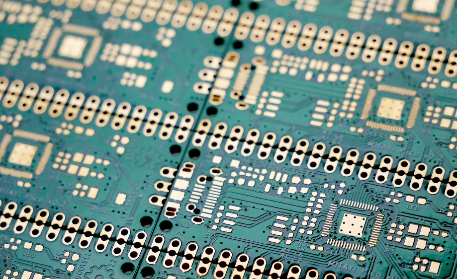
The Printed Circuit Board (PCB) is the structure that supports all electronic components and connects them electrically. It is made of conductive copper layers separated by insulating layers. Depending on complexity, a PCB can be single-sided, double-sided, or multilayer — with up to 20 layers for high-end designs.
Cutting and preparation
Production starts with large panels of composite material, most commonly FR4 (fiberglass reinforced epoxy). These panels are cut into optimized arrays to manufacture multiple boards simultaneously, saving time and materials.
Drilling
Computer-controlled drilling machines create hundreds of microscopic holes called vias, which connect layers together and form passages for through-hole components. These holes are then plated with copper to ensure electrical continuity between layers.
Copper deposition and etching
A thin copper layer is deposited over the entire surface. A photosensitive resist is applied and exposed to UV light according to the circuit pattern. After development, the unprotected areas are chemically etched away, leaving only the copper tracks — the electrical pathways of the circuit.
Solder mask, silkscreen, and finishing
After etching, the PCB is coated with a solder mask to protect traces and prevent short circuits. A silkscreen layer is then printed to identify components, references, and logos. Finally, a metallic finish (HASL, ENIG, or OSP) is applied to improve solderability and protect against oxidation.
Before shipping, every PCB is electrically tested. A “flying probe” test checks that all tracks are correctly connected and that no shorts exist. At this point, the PCB is ready for assembly.
3. Component soldering and assembly
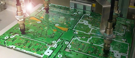
This stage transforms the bare PCB into a complete electronic board — the PCBA (Printed Circuit Board Assembly). The assembly process is performed on automated high-precision production lines.
Solder paste application
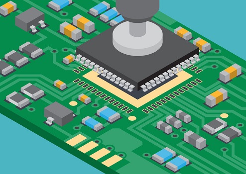
A layer of solder paste (a mixture of tin alloy, flux, and solvents) is deposited on the pads through a metal stencil. This paste will melt during the reflow process to form the solder joints.
Automated placement
High-speed pick & place robots position SMD (Surface-Mount Device) components at a rate of over 40,000 parts per hour. Each component is inspected by camera before placement to ensure accuracy and correct orientation.
Reflow and double-sided assembly
The assembled boards are then heated in a reflow oven following a specific thermal profile. The solder paste melts and solidifies, forming permanent joints. If components are placed on both sides, the process is repeated for the second side after temporary fixation of the first.
Through-hole soldering
Larger components (connectors, coils, or capacitors) require wave soldering or selective soldering. The PCB passes over a wave of molten solder that simultaneously connects all the pins.
A well-thought-out design can drastically reduce assembly costs. At AQ-Tech, our engineers apply a Design for Manufacturing (DFM) approach — every decision regarding components and layout is made to simplify production and maximize reliability.
4. Quality control and functional testing
The reliability of an electronic product depends directly on the quality of its inspections. Each assembled board undergoes several verification steps:
- AOI (Automatic Optical Inspection): high-resolution cameras check component presence, polarity, and alignment.
- X-ray inspection: used for BGA packages where solder joints are hidden under the component.
- Electrical tests: measuring voltages, continuity, and critical signals.
- Functional tests: programming the microcontroller, checking interfaces and sensors, and simulating real use conditions.
- Custom test fixtures: dedicated benches or pneumatic jigs designed for rapid and repeatable validation.
A robust design integrates Design for Test (DFT) principles early on, making quality control faster and more efficient without increasing production costs.
5. Best practices for reliability and cost control
A well-designed board is a board that’s easy to manufacture. Here are a few key recommendations:
- Plan component availability early — some parts may have several months of lead time.
- Avoid rare, obsolete, or non-standard components.
- Collaborate with your EMS partner as early as possible to align on manufacturing capabilities.
- Prefer SMD components over through-hole ones whenever possible.
- Consider heat dissipation and thermal constraints from the start.
At AQ-Tech, we consistently apply these principles to ensure our clients receive robust, reliable, and production-ready electronic boards.
6. Conclusion
Manufacturing an electronic board is a complex process combining mechanical precision, chemistry, and automation. From copper etching to final soldering, each step plays a key role in the product’s performance. Choosing a skilled EMS partner and involving your design office early in the project are the best guarantees of a reliable, durable, and industrially viable product.
Want to learn more? Explore our Electronics & Firmware, Industrialization, and Manufacturing pages, or contact our team to discuss your next project.
